AMD shared information about its future processors earlier at the Tech Day 2024 event, but the information published now goes into many details clearly more precisely.
AMD recently held a Tech Day 2024 event where it shared more details about its upcoming Zen 5 processors. However, not everything was told at that time, but now the company has published a number of additional slides to tell more about the inner life of its processors.
AMD’s new slides review the company’s entire upcoming Zen 5 product family and take a closer look at the features of the Granite Ridge and mobile-oriented Strix Point processors coming to the desktop. In addition to the above-mentioned circuits, Epyc processors of the Zen 5 architecture codenamed Turin are coming to the market. The Zen 5 architecture is designed for use with both 3 and 4 nanometer class processes.
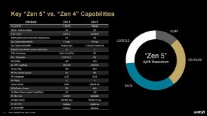
As learned in the last generation, AMD approaches energy-efficient and smaller cores from a different angle compared to Intel. AMD’s “Zen Dense” or c-marked versions offer the same features and IPC as the beefier Zen 5 cores, but with a smaller cache and clock speed, which help shrink the core. While the Zen 4c cores were up to 35% smaller than the Zen 4 cores, the size of the Zen 5c cores has been reduced by only 25%, at least this time around. However, an AMD representative has assured Tom’s Hardware that Zen 5c can be further shrunk for processors with only Zen 5c cores and that the current size was reached because it fits the intended use, i.e. Strix Point mobile processors. You can also find a detailed comparison between the Zen 4 and Zen 5 architectures above.
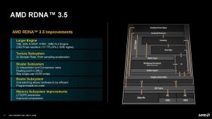
The changes to the RDNA 3.5 architecture used in Strix Points have been rather tight-lipped until now. Now the company has revealed that RDNA 3.5 has one larger Shader Engine than before, which now includes 8 WGPs, i.e. 16 CUs, four RB+ ROP units and “2 MB GL2 Engine”, which unfortunately is not a familiar expression to the undersigned . The texturing units are now capable of twice the sampling speed and point sampling has also been accelerated. In the shader units, interpolation and comparison tasks can now also be done at twice the speed, and the Scalar ALU now supports floating point numbers. Also, the graphics core no longer writes disposable data to the VGPR registers. The operation of the rasterization side has also been enhanced and the memory controller has received improved compression features and support for LPDDR5 memories.
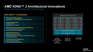
The same chip also has the XDNA 2 NPU or artificial intelligence accelerator. In the case of Strix Point, a package of four eight AI Engine cores is used, which has 1.6 times its own memory. According to the company, it can support at best 50 TOPS INT8 and 50 TFLOPS with Block FP16 resolution. At the same time, the execution can now have twice as many tasks, and the units support the Sparsity feature in addition to the new Block FP16. XDNA 2 is said to be at best twice as energy efficient as the first generation XDNA.
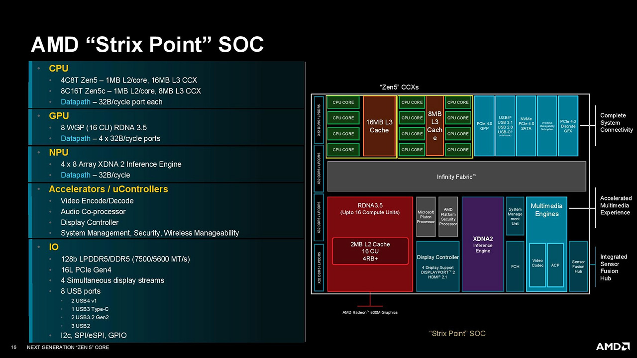
Whereas in Phoenix all processor cores were in one cluster, in Strix Point we switch to the tactic of two CCX; four Zen 5 cores and 16MB of L3 cache is one CCX and eight Zen 5c cores and 8MB of L3 cache is the other CCX. There are still only 16 PCIe lanes in total and they support PCIe Gen 4 speeds. In practice, this means that a possible side-by-side graphics card only gets eight lines, because some of the lines go to NVMe SSD drives. According to the company, the last four of the previous 20 lines were so little used that there was no longer a sufficient need for them.
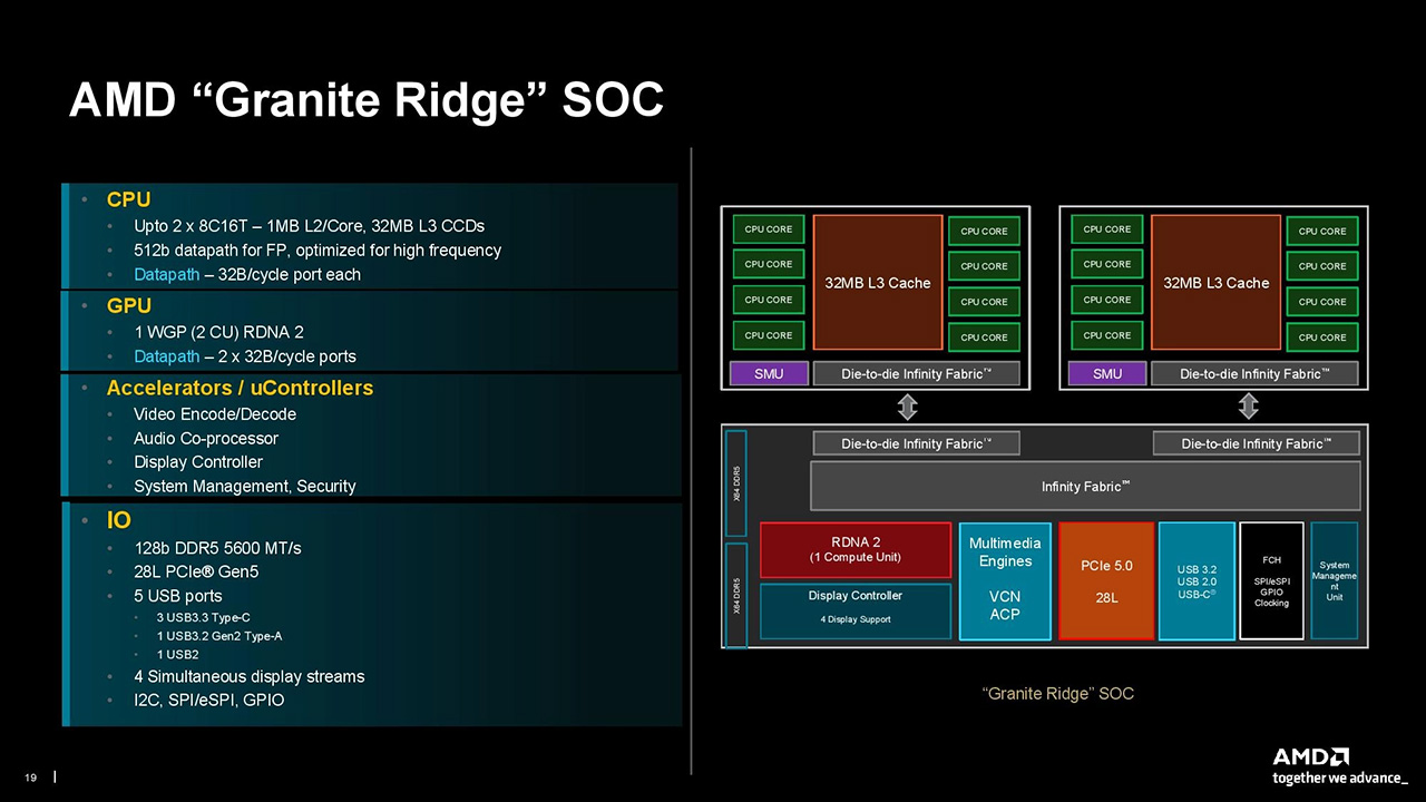
On the desktop side, Granite Ridge exclusively has Zen 5 cores split into two CCD chips with eight cores and 32 MB of L3 cache. The CCDs are connected to the IO chip familiar from the Ryzen 7000 series, which, contrary to some claims, still includes the graphics controller of the RDNA 2 architecture 2 Compute Unit. There are also the familiar 28 PCIe 5.0 lines, some of which are reserved for the chipset connection.
Source: AMD, Tom’s Hardware
Source: www.io-tech.fi


