
Joint research team improves blue phosphorescent OLED power efficiency by 24% and stability by 21%
Development of Intermediate Layer with Lower OLED Driving Voltage… Lowering the Threshold for Commercialization, Published in ‘Chem’
A new organic semiconductor material has been developed that can significantly improve the luminous efficiency and stability of blue OLEDs (organic light-emitting diodes).
It is expected to accelerate the commercialization of next-generation high-purity, high-efficiency display technology.
The research team of Professor Taehyuk Kwon and Professor Wonyoung Choi from the Department of Chemistry at UNIST (President Jong-Rae Park), in collaboration with the research team of Professor Junyeop Lee from Sungkyunkwan University, has developed a new interlayer material that can solve the lifespan issue, which was the biggest challenge for blue phosphorescence OLEDs.
Research team. (Clockwise from left on top row: Professor Kwon Tae-hyeok, Professor Choi Won-young, Researcher Kim Ji-yeon, Researcher Hwang Eun-hye (first author), Researcher Kim Min-seok)
View Original Icon
The developed material significantly reduced the OLED driving voltage compared to existing ones. Power efficiency was improved by 24%, and driving stability was improved by 21%. It showed the possibility of being applied not only to blue OLEDs as an intermediate layer, but also to next-generation inorganic-based light-emitting elements.
Phosphorescent OLED technology uses a luminescent mechanism that utilizes triplets to emit light more efficiently and for longer. Red and green phosphorescent OLEDs have already been commercialized, but blue phosphorescent OLEDs are difficult to commercialize due to their high operating voltage and short lifespan.
The research team developed a new intermediate layer that lowers the operating voltage of blue OLEDs and reduces light loss. The existing twisted molecular structure was effective for triplet confinement, but had limitations in current flow. The new material improved this and increased stability.
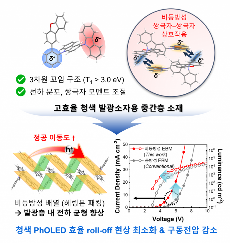
Anisotropic array-based organic semiconductor material design strategy.
View Original Icon
The research team created an anisotropic array by controlling how the charge moves and the properties of the material, improving the evenness of the electric flow while preventing light loss.
“It is highly unusual to implement a herringbone arrangement in a twisted molecular structure,” said first author Eunhye Hwang, a researcher. “This will be an important turning point in the development of new organic semiconductor materials.”
Professor Kwon Tae-hyuk said, “We have presented a new strategy for developing intermediate layer materials that simultaneously resolve triplet confinement and charge balance independently of the light-emitting layer,” and added, “Based on this, we plan to further intensify our research on next-generation displays and light-emitting devices.”
The research results were published on September 19 in the international academic journal Cell and its sister journal Chem. The research was supported by the National Research Foundation of Korea (NRF), the Korea Institute of Energy Technology Evaluation and Planning (KETEP), and UNIST.
Yeongnam News Headquarters Reporter Kim Cheol-woo sooro97@asiae.co.kr
<ⓒ투자가를 위한 경제콘텐츠 플랫폼, 아시아경제(www.asiae.co.kr) 무단전재 배포금지>
Source: www.asiae.co.kr
